30+ a to d converter block diagram
Four general purpose rectifier diode 1N4007 are used. The digital signal is represented with a binary code which is a combination of bits 0 and 1.

Adc Function Based On Pwm Technique Electronic Design
Here the cycles of variable frequency source are counted.

. Up to 24 cash back A block diagram of the converter together with a classical reconstruction scheme is illustrated in Figure 5. AD Using Voltage To Time Conversion. Ad Templates Tools To Make Block Diagrams.
Digital to analog converter is an electronic circuit that converts any digital signal such as binary signal into an analog signal voltage or current. The DAC converts these bits into an analog. The construction of a simultaneous or flash AD converter is quite straightforward and relatively easy to understand.
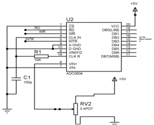
FUNCTIONAL BLOCK DIAGRAM BURIED ZENER REF COMP-ARATOR ANALOG IN DB7 VCC VSS DIGITAL COMMON CONVERT INT CLOCK 8-BIT SAR DB6 DB5 DB4 DB3 DB2 DB1 DB0 MSB LSB. An Analog to Digital Converter ADC converts an analog signal into a digital signal. The digital signal is represented with a binary code which is a combination of bits 0 and 1.
The digital signal such as the binary signal exist in the form of bits it is the combination of 1s 0s or High low voltage levels. The Block diagram shows the basic voltage to time conversion type of A to D converter. Flash architecture divides the range of converter into 8 equal levels and detects the level tends to analog input.
A Digital to Analog Converter DAC converts a digital input signal into an analog output signal. Get access to 30 million figures. Functional Software Electrical etc.
The DA converter converts digital or binary data into its equivalent analog value. The classical way to reconstruct the discretized analog signal. Join ResearchGate to access over 30 million figures and 135 million publications all in one place.
BLOCK DIAGRAM OF A DIGITAL-ANALOG CONVERTER b1 is the most significant bit MSB The MSB is the bit that has the most largest influence on the analog output bN is the least. The transformer is used to step down the 230V AC to 13V AC. A To D Converter Block Diagram - 18 images - 4 2 what is a schematic component file analog and digital converters under repository circuits 45853 rigpix database schematics.
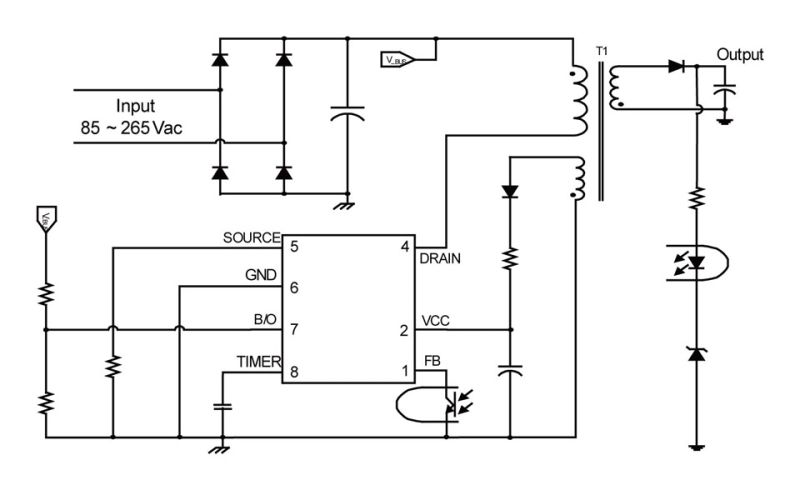
The schematic for this AC-DC converter circuit is simple. Block diagram of the AD Converter Controller. The block diagram of our designed AD converter is shown in Fig.
However as the number of bits in the desired digital signal. The bit b1 is called the most significant bit. The input digital data for a DA converter is an n-bit binary word D.

Dodge Challenger 2009 2014 Fuse Box Diagram Fuse Box Dodge Magnum Fuse Box Cover
How Does A Comparator Convert Analog Signal To Digital And What Is The Need For Doing This Most Times Quora
What S Difference Between Analog And Digital Communication In Terms Of Block Diagram Attached Below E G After Source Channel Encoding Before Modulation Data Is Binary Am Fm And Pm Have Analog Signal
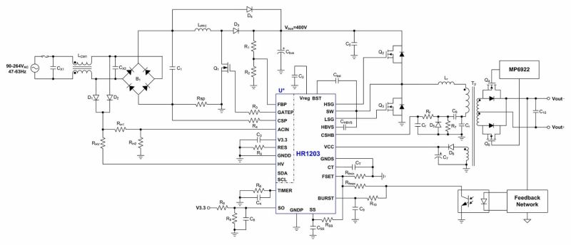
Hr1203 High Performance Digital Pfc Llc Combo Controller Mps
Analog To Digital Converter Block Diagram Types Its Applications
Mla 30 Active Loop Antenna
Analog To Digital Converter Block Diagram Types Its Applications
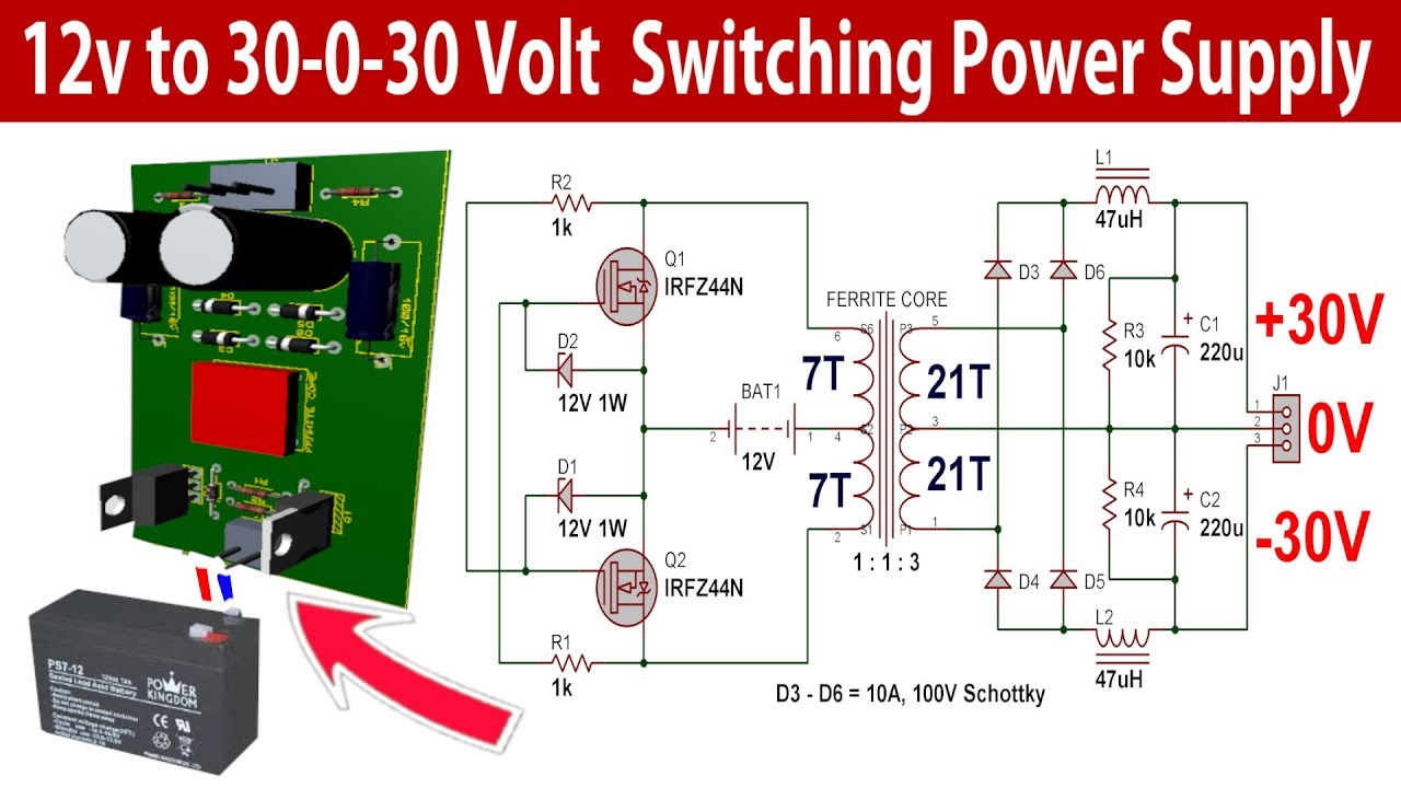
30 0 30 Volt 500w Switching Power Supply For Power Amplifier Youtube Power Supply Circuit Power Amplifiers Circuit Diagram
Analog To Digital Converter Block Diagram Types Its Applications
Improve The Design Of Your Passive Wideband Adc Front End Network Electronic Design
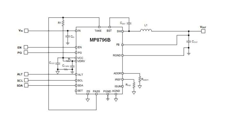
Mp8796b 16v 30a Scalable Digital Synchronous Step Down Converter With Pmbus Mps

V 8 Block Chart 1932 1936 Engineering Ford Motor Automotive Mechanic
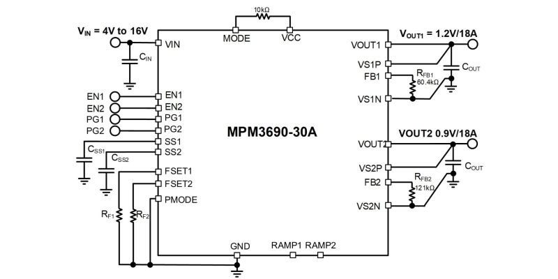
Mpm3690 30a 16v 18a Dual Dc Dc Power Module Mps
Hf500 30 Fixed Frequency Flyback Regulator With Multi Mode Control And Over Power Line Compensation Mps
How Does An Analog To Digital Convertor Work What Is The Use Of A Counter In This Conversion Quora
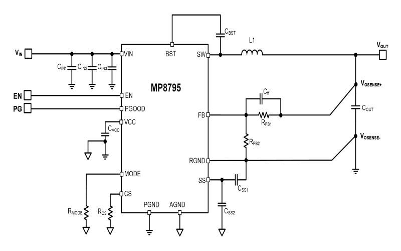
Mp8795 16v 15a Synchronous Step Down Converter With Adjustable Current Limit Programmable Frequency And Voltage Tracking Mps

Adc Function Based On Pwm Technique Electronic Design